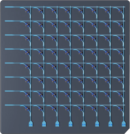
PCM+Crossbar approach
Electrical pulse modulation of phase-change material state with delay at nanosecond level.

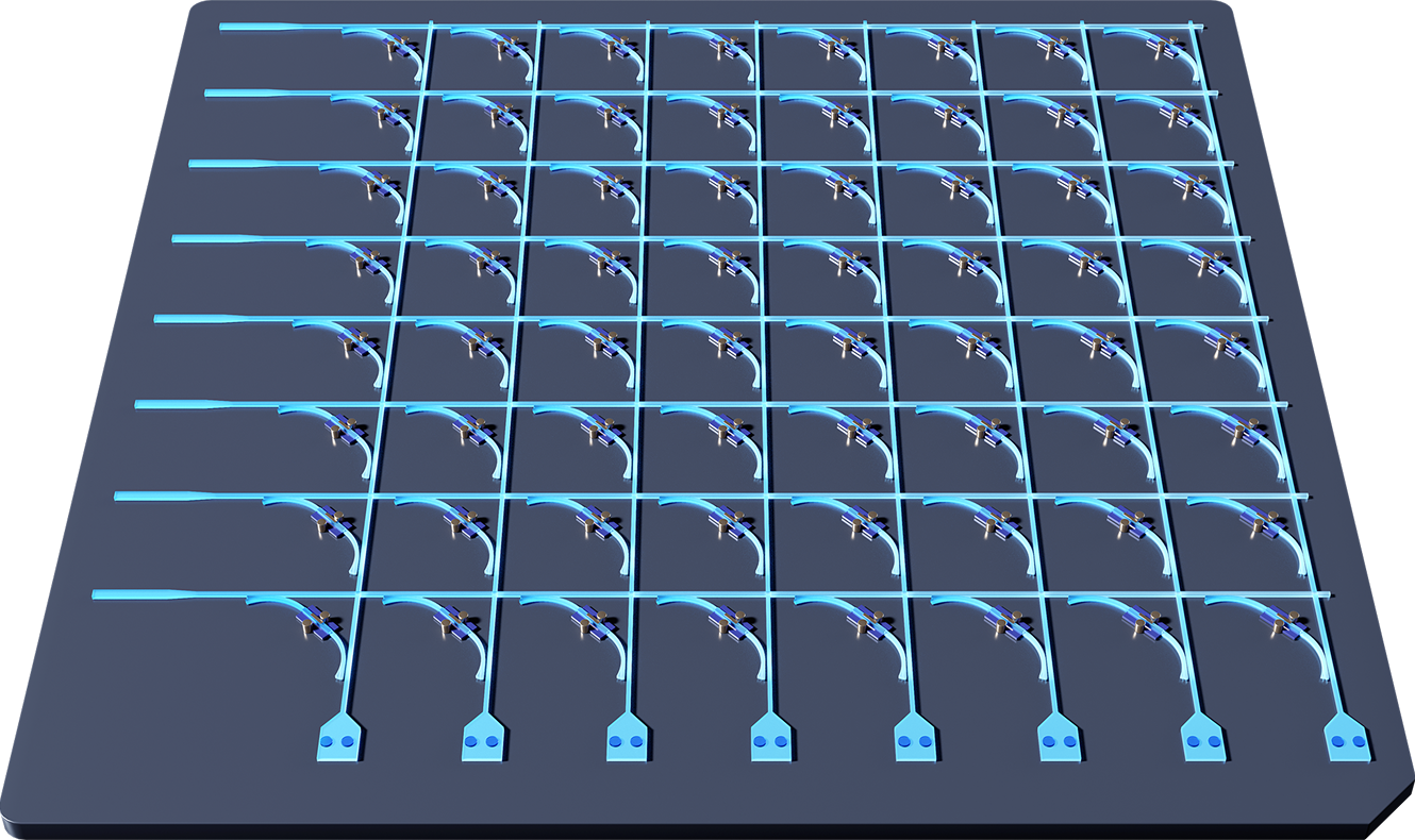
Silicon-Photonics PCM Heterogeneous
Integration + Crossbar Photonic Matrix
Silicon-Photonics PCM Heterogeneous
Integration + Crossbar Photonic Matrix
Silicon-Photonics PCM Heterogeneous
Integration + Crossbar Photonic Matrix
Route Overview
Route Overview
Route Overview
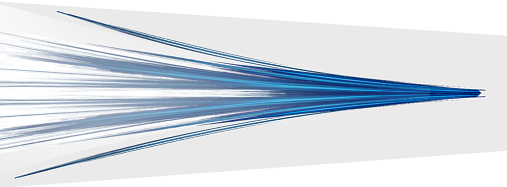
Lightstandard adopts a technical approach based on heterogeneous integration of silicon photonics and phase-change materials, combined with a Crossbar photonic matrix computing architecture. By modulating the state of phase-change materials, we control the transmittance of light in waveguides containing phase-change materials. The incident light power and the phase-change material state can be mapped as multiplier and multiplicand respectively, and the power value of light after passing through the waveguide containing phase-change materials can be read as the product. Multiple product light beams converge into a single beam through coupling, and the power value of this beam represents the result after addition. Through the Crossbar (matrix cross) structure, multiple incident light beams can simultaneously perform multiplication and addition operations, thereby achieving matrix multiplication. Compared to other optical computing technical approaches, this approach enables in-memory computing with optical chips, offering advantages such as small unit size and low system power consumption.
Limited Size,Low Array Count,Complex Packaging
Limited Size,Low Array Count,Complex Packaging
Limited Size,Low Array Count,Complex Packaging
Small Size, High Integration, Easy Packaging
Small Size, High Integration, Easy Packaging
Small Size, High Integration, Easy Packaging
Zero Static Power Consumption, High Stability
Zero Static Power Consumption, High Stability
Zero Static Power Consumption, High Stability

High Modulation Speed, High Computing Efficiency
High Modulation Speed, High Computing Efficiency
High Modulation Speed, High Computing Efficiency

What industries are optical computing solutions best suited for?
What are the primary technical approaches in optical computing?
What are the advantages of optoelectronic fusion computing cards?
What emerging materials are utilized in optical computing chips?
What packaging architectures are available for optoelectronic fusion computing cards?


What industries are optical computing solutions best suited for?
What are the primary technical approaches in optical computing?
What packaging architectures are available for optoelectronic fusion computing cards?