Written by CCF Task Force Executive Committee Member Yao Jinxin,
Special Contributor for Tencent Tech.
Edited by Guo Xiaojing.
At GTC 2025, NVIDIA continued its "computing power story." If AI development continues to follow the scaling law, this story can continue. However, the reality is that while the core framework of "non-sleep computing power" remains unchanged, the underlying technical architecture is quietly undergoing a transformation. While the industry's attention is still focused on the performance breakthrough of the Blackwell Ultra GPU, the brief technical announcement in the presentation—"integrating silicon photonics technology directly into switch chips"—actually contains the key secrets to the evolution of AI infrastructure.
1
What exactly is Nvidia's CPO?
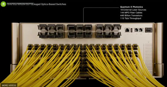
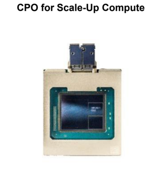
During Jensen Huang's keynote speech at the GTC conference, NVIDIA announced the Spectrum-X and Quantum-X silicon photonics CPO switches.
These two products support configurations of 144×800G (launched in H2 2025) and 512×800G (launched in H2 2026), aiming to meet the urgent needs of AI supercomputing for high bandwidth and low power consumption.
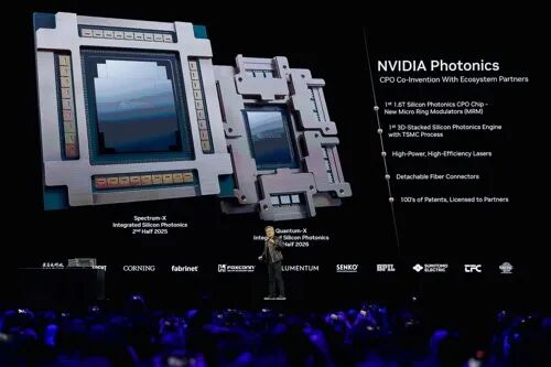
§ Spectrum-X Photonics: Ethernet switches offering up to 512 800Gb/s ports or 2,048 200Gb/s ports, with a total throughput of up to 400Tbps.
§ Quantum-X Photonics: InfiniBand switch, providing 144 800Gb/s ports based on 200Gb/s SerDes, with a total throughput of 115.2Tbps.
According to the information provided in the keynote, these switches offer significant advantages over traditional solutions:
§ The overall number of lasers in the system was reduced (75%).
§ Achieved a 3.5-fold reduction in energy consumption.
§ Network resilience is increased 10 times, significantly enhancing reliability and ensuring uptime.
§ Deployment speed increased by 1.3 times
§ Signal integrity increased by 63 times
2
Opening the door to a million-GPU AI factory
At the press conference, Huang's original words were: "NVIDIA has integrated silicon photonics directly into the switch, breaking the old limitations of hyperscale and enterprise networks and opening the door to a million-GPU AI factory."
"Under the guidance of the Scaling Law, continuously increasing the scale of computing power has become an industry consensus. From a system perspective, expanding the scale of computing power has two dimensions: one is to improve the computing power of chips; the other is to increase the number of chips in the system, that is, to increase the cluster size. This can be done in two ways: horizontal scaling (Scale-Out) and vertical scaling (Scale-Up).
1) In the first case, the performance improvement of single-chip computing power is mainly affected by two factors: computing power (density) and memory bandwidth. To achieve a significant improvement, efforts need to be made in high-end process technology.
For example, a 3nm chip has a much higher computing power density than a 12nm chip of the same area, and HBM has a much higher bandwidth than traditional DDR. These are all closely related to manufacturing capabilities.
For fabless AI chip companies, computing power is essentially about manufacturing processes. It's no longer about how cleverly they design their architecture; it's about competing for, or even leading, top-tier manufacturing capabilities. Even if these limitations can be overcome, the advancement of advanced manufacturing processes for silicon chips based on electronic computing still faces physical constraints (this is important and will be discussed later).
2) The second type is to increase the cluster size. Horizontal scaling (Scale Out) refers to expanding beyond the size limit, while vertical scaling (Scale Up) refers to increasing performance proportionally.
§Horizontal scaling: This can be understood as distributed computing, increasing computing capacity by adding independent servers to distribute the workload. In AI clusters, this can be compared to what InfiniBand or RoCE networks do.
§Vertical scaling focuses on upgrading single servers or chassis-based systems by adding chips to existing systems to increase computing power. This can be compared to what NVLink does in AI clusters.
It can be seen that the essence of improving the computing power of a large-ale cluster is in-volume communication technology;
3
What problem does the CPO actually solve?
In this way, communication and networking technologies within the cluster become key elements for improving system computing power.
In traditional solutions, the most important elements are two points and one line: the two points refer to the network chips (cards) and switches at both ends of the communication, and the line refers to the optical transmission system, which includes optical modules and optical fibers. Signal transmission occurs in the optical fiber and is connected to the switch via optical modules.
In traditional optical communication architectures, as switch bandwidth increases, total link power consumption also increases rapidly. See the diagram below.
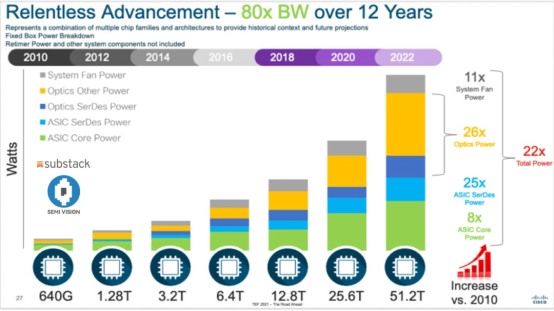
Increased link speeds not only mean increased power consumption, but also greater technical challenges in ensuring signal integrity (SI), significantly increasing the challenges of technological advancement, as shown in the figure below:
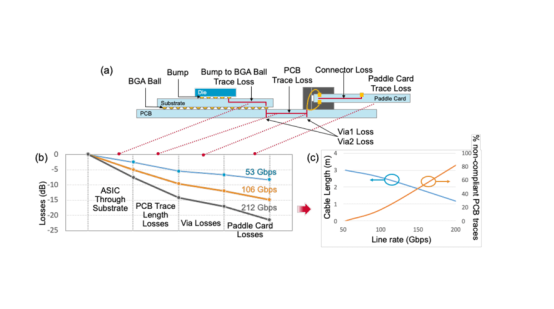
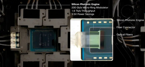
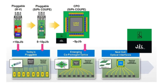
Considering that both the DSP in the optical module and the ASIC in the switch are electrical chips, transferring some functions of the DSP to the ASIC can eliminate the need for the DSP, thereby reducing power consumption. On the other hand, if the distance between the optical chip in the optical module and the electrical chip (ASIC) in the switch is shortened enough to be integrated onto a single chip, then the signal integrity issue is resolved. See figure.
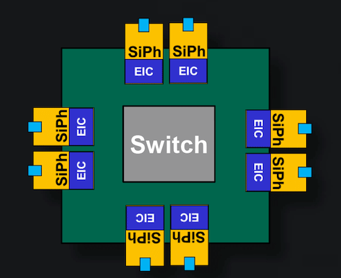
The emergence of Co-Packaged Optics (CPO) was precisely to solve these problems. It offers significant advantages compared to traditional DSP-based pluggable optical modules.
CPO integrates optical components directly with the ASIC, eliminating the need for a DSP chip and migrating its functionality to the ASIC (switch chip in a switch). This integration effectively reduces power consumption and improves efficiency and overall performance. By removing the DSP from the optical module and integrating the optical chip with the switch ASIC chip, the transmission distance between the two is significantly shortened. CPO reduces latency and power consumption during signal conversion, making it a more scalable and energy-efficient solution for high-speed data transmission. The figure illustrates the improvements in power consumption and latency based on TSMC processes under pluggable and CPO configurations.
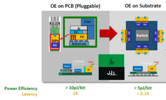
In short, the CPO switch released this time has removed the optical module, allowing the fiber optic connector to be directly connected to the switch.
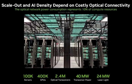
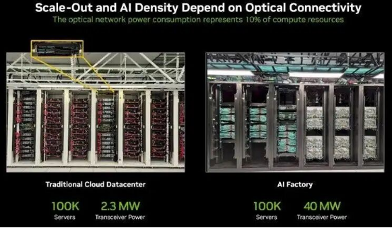
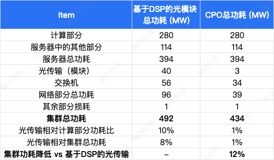
For a typical "AI factory" as shown in the diagram above, taking 400K GPUs as an example, the main power consumption data is shown in the table below:
4
The entry of tech giants into AI computing will bring about change
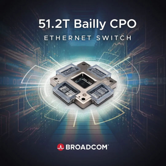
In fact, Nvidia is not the first company in the industry to release a CPO switch. Previously, Broadcom took the lead in releasing 25.6T and 51.2T CPO switch chips and launched corresponding CPO switches with other manufacturers in the industry.
Marvell has also launched a CPO solution for Teralynx®. Cisco previously released a 25.6T CPO switch.
The official launch of NVIDIA's CPO solution today is significant because it marks the commercialization of NVIDIA's product, making it a leading global manufacturer of data center chips, following Broadcom and Marvell, two giants in communication chips and AI ASIC customization. These industry leaders wield immense influence, and their investments and product iterations in silicon photonics and optoelectronics will significantly contribute to the development of the silicon photonics and optoelectronics industry, ultimately leading to the optical transformation of computing systems.
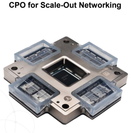
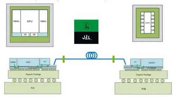
At this point, its significance extends beyond just switches. Silicon photonics-based optoelectronic packaging will expand from CPO (Content-Based Programming) for switching to GPUs or other AI computing chips, further improving communication performance between computing chips. The diagram illustrates Broadcom's horizontally scalable CPO solution based on network switching and its vertically scalable CPO solution based on AI computing cores.
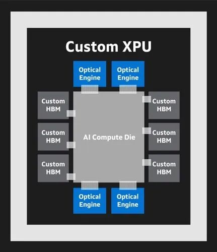
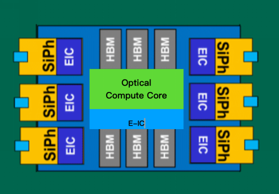
In fact, if the same approach is applied to scale-up computing—that is, integrating AI chips and optical chips onto a single chip—the interconnectivity between AI chips will significantly improve transmission bandwidth, reduce power consumption, enhance signal integrity, and greatly expand the number of nodes. Taking NVIDIA as an example, if a GPU+SiPh (silicon photonics) CPO can be achieved, it can increase NVLink bandwidth and expand the number of GPUs that can be connected, potentially exceeding 288. This heterogeneous integration of the GPU's electro-computing silicon chip and the optical-based silicon photonics chip is the CPO for AI computing. As shown in the figure, the energy consumed per bit transmitted is lower, and the latency is shorter.
From an interconnect perspective, the industry refers to this solution as OIO (Optical I/O). The new GPU architecture announced at GTC is called Rubin, and the next generation will be Feynman, expected to launch in 2028. At that time, the Feynman-based architecture will be a new chip with OIO capabilities.
§ Silicon Photonics will replace copper interconnects.
§ The world's first 1.6T silicon photonics-based optical interconnect interface
§ The GPU/NVSwitch will implement optical interconnects, as shown in the figure:
5
What is its significance and impact on China?
In recent years, the geopolitical landscape has become increasingly uncertain, and technological restrictions have become commonplace. For my country, computing chips based on electronic computing have consistently faced technological limitations in advanced manufacturing processes and packaging. Since 2022, the U.S. Department of Commerce has been introducing restrictions annually, from early limitations on computing density, computing power limits, and interconnect bandwidth, to later limitations on transistor count, chip area, and manufacturing processes, and most recently, the implementation of a whitelist system. The path forward for China's computing chips is fraught with difficulties. Countless industry elites have dedicated themselves to this field; enormous amounts of capital have been invested; and now, a glimmer of hope seems to emerge, but production capacity remains scarce; advanced technologies and processes still require further development.
Optical computing and optical transmission offer another hope.
As mentioned earlier, improving the computing power of computing chips themselves, if still based on silicon-based computing dies (Si-Compute Dies), will face physical limitations. From a technical feasibility perspective, optical-based computing dies represent a new direction for improving the energy efficiency of computing power. When the computing dies in AI chips are replaced with optical computing dies, this new type of optoelectronic co-packaged chip based on optical computing dies + OIO (Optical In-line Interchange) will become a very important technical route and product solution.
This new form of AI computing chip represents a strategic high ground in the next stage of computing power competition.
The fabrication of silicon photonics chips doesn't place particularly high demands on fabs; DUV lithography machines are sufficient, and even more imaginative product forms can be achieved using alternative methods. Based on accumulated expertise in traditional electronic chip packaging technology, breaking through the limitations of optoelectronic encapsulation is not significantly more difficult than with traditional electronic chips. From this perspective, the trend brought about by CPO (Contract Production Organization) is favorable to my country. In the field of optical communications, China boasts world-leading optical module and chip manufacturers, and domestic companies also hold a high market share in the switch sector. The silicon photonics industry has also received increased attention in the past year or two, and the construction of silicon photonics production lines is booming.
However, we must acknowledge the gap. As mentioned earlier, the leading companies in this field are still traditional giants like Broadcom, NVIDIA, and Marvell, who are driving the development of the industry and technology. On the manufacturing side, TSMC, as a high-end manufacturing giant of traditional silicon chips, also announced its COUPE solution for optoelectronic co-packaging in 2024, giving it a leading edge at present.
More importantly, the United States began paying close attention to the development of China's silicon photonics industry last year, indicating that it would implement restrictive policies. On October 28, members of Congress from both parties urged the U.S. Department of Commerce to review the threat posed to U.S. national security by China's development of silicon photonics technology. They stated that silicon photonics technology is a rapidly developing field that can accelerate the advancement of artificial intelligence.
But as dawn breaks, the light of day is breaking. In the competition within the AI industry, staying in the game is the most important strategic goal. While China is striving to catch up in the era of electronic chips, and with a better start in optical chips, it cannot and will not fall behind.
Recommended News
Recommended News
Recommended News