Author | Wu Ruoyu
Edited by Peng Xiaoqiu
In 2022, two young people under the age of 30—one shutting down his American company and the other pausing his doctoral studies at Oxford University—returned to China to found a company called "Lightstandard".
Three years later, Lightstandard has completed the tape-out of the world's first optical computing chip with computing power density and accuracy reaching commercial standards, becoming the only optical computing chip company in the world to achieve in-memory computing integration and integrate 128*128 matrix-scale optical chips onto a single die.
The person who shut down the US company is Xiong Yinjiang, co-founder and chairman of Lightstandard, who is now in charge of operations and commercialization. He has a master's degree from the University of Chicago and has many years of practical experience in engineering large model algorithms and AI agents. The person who suspended his doctoral studies is Cheng Tangsheng, co-founder and CEO of Lightstandard, who is now in charge of R&D and engineering implementation. Cheng Tangsheng was once a student of Harish Bhaskaran, the world's first person in "phase change material optical computing" and a Fellow of the Royal Academy of Engineering.
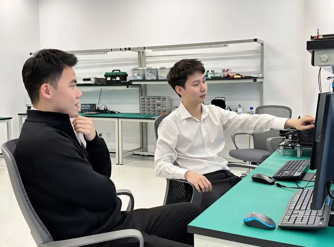
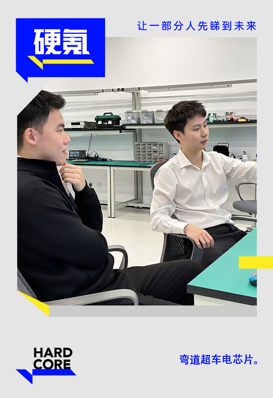
The two co-founders of Lightstandard are Xiong Yinjiang (left) and Cheng Tangsheng (right).
Xiong Yinjiang and Cheng Tangsheng decided to take a gamble on starting their business because they had been focusing on opportunities in the field of optical computing for many years. Before starting their venture, they had already completed the tape-out and application verification of small matrix chips such as 3×3 and 4×4, accumulating experience across the entire process, including tape-out, design, and materials. The explosive growth in AI demand in 2022, coupled with the potential to revolutionize chip manufacturing using the speed and advantages of light, seemed to offer a real breakthrough in Moore's Law and alleviate computing power anxiety. They felt the perfect time had arrived. Especially this year, with the further rise of large-scale models and generative AI, the industry's demand for computing power has exploded. Not only model training itself, but also subsequent practical inference stages, have led to even higher energy consumption.
According to the International Energy Agency's "Energy & AI" report, global data centers consumed approximately 415 terawatt-hours of electricity in 2024, accounting for 1.5% of global electricity consumption. This figure is projected to more than double by 2030, reaching approximately 945 terawatt-hours, exceeding Japan's current total electricity consumption.
Meanwhile, the computing power of a chip is directly linked to the number of transistors it contains. Currently, the 3-nanometer lithography process is approaching the atomic physical limit of 0.3 nanometers. To further improve the computing performance of electronic chips in terms of manufacturing process, the only way is to continue Moore's Law through advanced packaging such as stacking. However, this is only a weak support and cannot solve the contradiction between energy consumption and computing power supply and demand in the long run.
Since 2017, academic discussions on optical computing by Oxford University and MIT have attracted attention both at home and abroad. People have discovered that in addition to stacking chips and transistors like building a skyscraper from scratch, optical chips can perform signal processing using optical technology, and have the potential to improve computing power by more than 1,000 times compared to electrical chips, while consuming less energy and having a wider bandwidth.
In recent years, in addition to the attention paid to the progress of optical computing chips by governments, capital markets, and computing power ecosystem companies, many optical computing chip companies have emerged both at home and abroad. Lightstandard was established against this backdrop, focusing on the research and development of photonic in-memory computing chips based on heterogeneous integration of silicon photonics and phase change materials (PCM).

From laboratory to commercial application
To move optical computing chips from the laboratory to industrial applications, two key challenges need to be overcome: first, how to miniaturize light from the fiber optic scale to the chip scale; and second, while achieving size miniaturization, retaining the chip's ability to handle complex computing tasks to ensure it meets the actual needs of scenarios such as large models and intelligent computing centers.
The breakthrough of Lightstandard began with a precise judgment of the timing of entry. "In 2017, although optical computing chips attracted attention due to their many advantages, the industrial chain links such as domestic and foreign fab manufacturing and packaging processes were not yet mature. In particular, the shortcomings in key processes such as chip packaging made it difficult to promote the commercialization of optical computing chips," said Xiong Yinjiang, co-founder and chairman of Lightstandard.
By 2022, the AI boom and the gradual maturation of the entire industry chain presented a crucial opportunity for design companies to take the initiative and accelerate the iteration of the production chain through demand-driven growth, thus expediting commercialization. Therefore, Lightstandard chose this moment to enter the market.
Compared to the typical pace of technology companies, the productization process of Lightstandard solutions is progressing significantly faster.
After its establishment, the company quickly completed iterations of matrix sizes such as 16x16 and 25x25. In 2023, it achieved tape-out of a 64x64 matrix, and in June of the following year, it achieved a breakthrough in a 128x128 matrix.
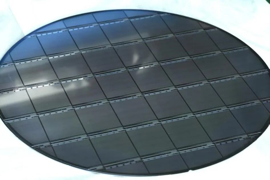
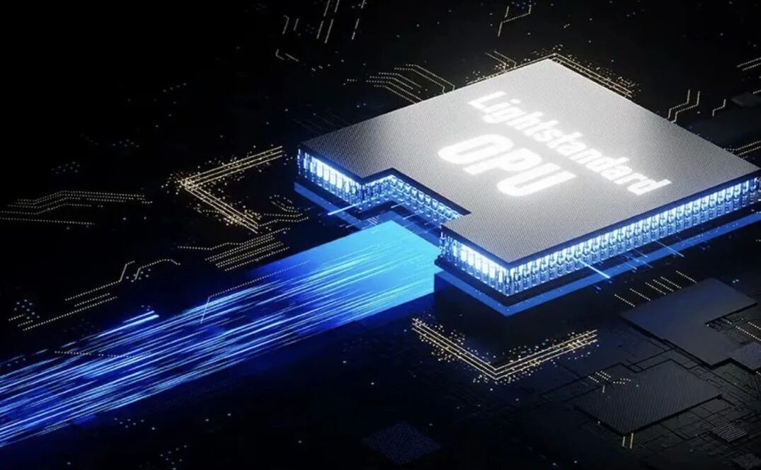
128*128 matrix-scale optical computing chip
However, the 128×128 matrix tape-out is only the first step towards commercialization. "Simply using matrix numerical values cannot build a moat. Many solutions have fixed node values, which can only be used for specific calculations and cannot be adapted to different models," Xiong Yinjiang emphasized. The value of the Lightstandard chip also lies in creating the first architecture with "16,000+ nodes and each node being fully adjustable".
For scenarios such as large models, 128×128 is the current "economically feasible" scale for model splitting, while the real-time adjustability of nodes allows the chip to adapt to parameter changes of any model, opening up key space for the programmability of matrix operations - this is the core sign that optical computing chips have moved from scientific research to commercial use.
Supporting this breakthrough is the unique choice of technology route by the Lightstandard approach: heterogeneous integration of silicon photonics and phase change materials, as well as the unique Crossbar photon matrix computing structure, which provides the core solutions to the two problems of "scale miniaturization" and "computing power and energy consumption balance".
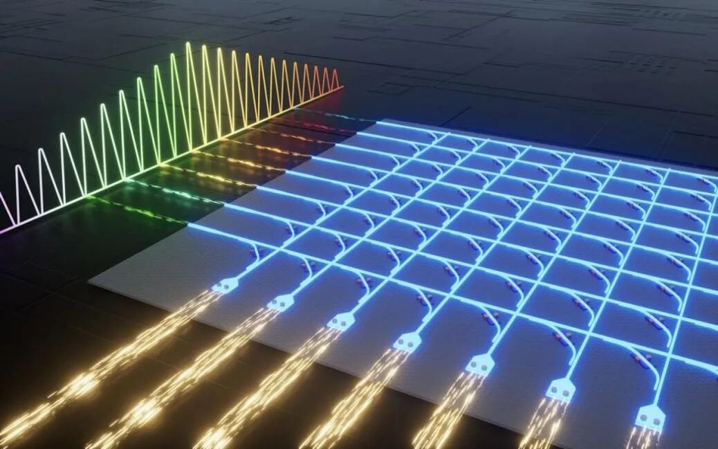
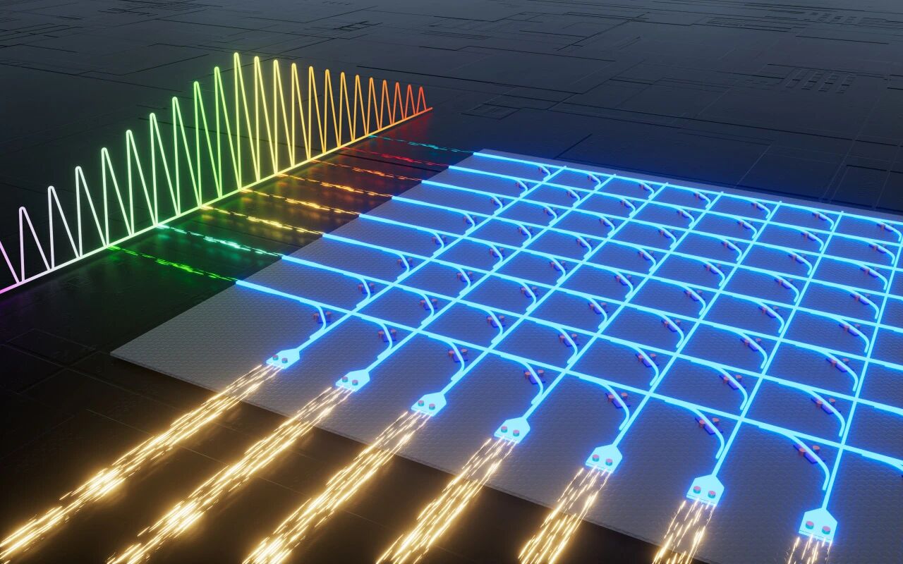
Crossbar technology roadmap demonstration
“Traditional pure silicon architecture programmable computing units are large in size, with a maximum of several hundred units placed on a standard chip area. At a standard GHz clock speed, the computing power is only a single-digit TOPS, which is far from meeting the needs of AI. More importantly, pure silicon materials require continuous power supply 24 hours a day to maintain their state during computing, and this part of the power consumption accounts for 70-80% of the total power consumption of the system, which puts forward very high requirements for heat dissipation and runs counter to the trend of explosive growth in computing power demand,” Xiong Yinjiang explained.
Through research, the Lightstandard approach utilizes phase change materials to reduce the unit size to 1/10 to 1/20 of traditional solutions, increasing the matrix size that can be accommodated by 10 to 20 times. Regarding the energy consumption of AI chips, the Lightstandard approach also made optimizations during the design phase.
Today, chips based on heterogeneous integration of silicon photonics and phase change materials can complete parameter refresh with only a single pulse of extremely low energy. Furthermore, due to the non-volatile nature of phase change materials, no continuous energy is required to maintain the state, achieving near-zero power consumption.
Furthermore, based on the storage function of PCM phase change materials, the Lightstandard chip integrates the storage unit and the computing unit, realizing in-memory computing, further alleviating storage pressure and improving chip performance.

How do you sell optical chips?
Entering the commercialization stage, the requirements for technology companies become more pragmatic. Currently, the two types of cloud-side customer groups targeted by Lightstandard have significantly different but clearly defined needs.
The end-users, represented by major internet companies, are also the "final battleground" in the computing power ecosystem. These customers possess mature computing clusters and large-scale model development capabilities. For them, if optical computing chips can significantly outperform in core indicators such as energy efficiency and computing density, even with high initial investment, it has clear commercial viability. Furthermore, the rapid iteration of models requires hardware to be "ahead of software" and compatible with the next-generation software ecosystem.
Another type of cloud-side customer is government-led intelligent computing centers, whose needs are relatively standardized and who place greater emphasis on the economic benefits of projects. The difference in demands between these two types of customers is essentially a manifestation of the technological value in different scenarios, which precisely constitutes the complete market coordinate system for optical computing chips from technology verification to large-scale commercialization.
The optoelectronic fusion computing card being developed by Lightstandard can use PCIe interface or other common standards for data interaction. It is plug-and-play and provides easy-to-use upper-layer application interfaces and ecosystem. It has high energy efficiency, high algorithm flexibility and is suitable for different application scenarios.
“In the future, our products will also be validated in edge scenarios, where the differences in customer needs between cloud and edge scenarios will be even greater. The core requirements for cloud scenarios are high energy efficiency and algorithm flexibility, requiring significant investment in software ecosystem building and targeted optimization of hardware and algorithm compatibility; edge scenarios emphasize stability, especially automotive-grade applications which need to cope with complex environments such as extreme temperatures, placing higher demands on hardware reliability,” added Cheng Tangsheng, co-founder and CEO of Lightstandard.
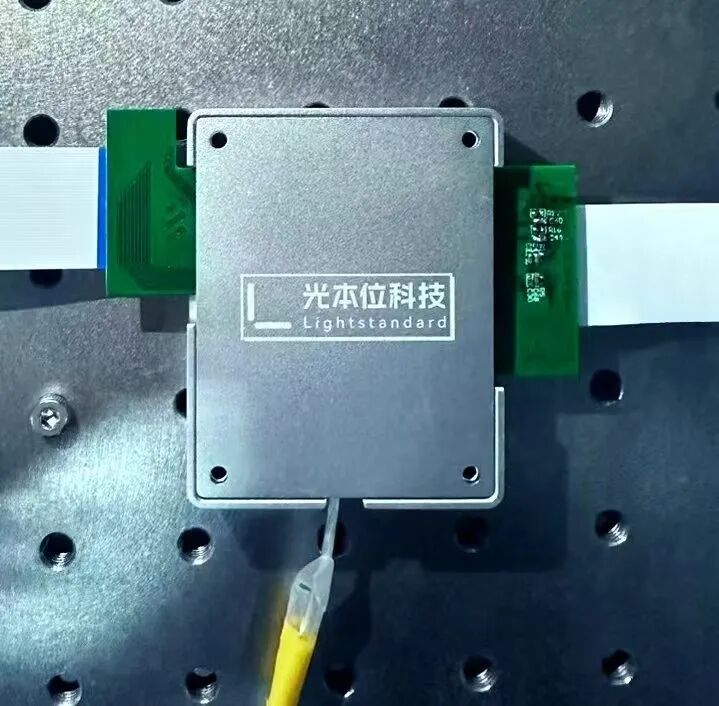
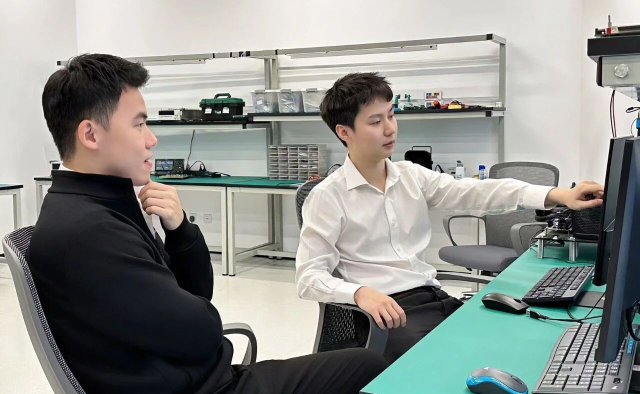
Photonic AI computing demo hardware with initial packaging completed
Currently, Lightstandard has established partnerships with leading domestic internet companies, GPU manufacturers, intelligent computing centers, and universities, awaiting further application verification. At the same time, it is also engaging in in-depth technical exchanges with satellite manufacturers, telecommunications operators, and optical module manufacturers regarding applications.
In terms of packaging and testing, Lightstandard has long established partnerships with fab manufacturers, jointly developing advanced packaging processes and driving technological iteration. This year, Lightstandard will complete the packaging and testing of a 128×128 matrix optical computing chip and electrical chips, forming the first-generation optoelectronic converged computing card. At the same time, it will advance the tape-out of a 256×256 matrix optical computing chip, and expects a more competitive second-generation optoelectronic converged computing card to be launched in 2026.
As its new product launch coincided with the completion of another round of financing in June of this year, led by Dunhong Asset Management, with follow-on investments from state-owned funds such as Pudong Science and Technology Angel Fund of Funds, Suzhou Future Angel Industry Fund, and Zhangjiang Science and Technology Investment, and existing shareholder Zhongying Venture Capital also increasing its investment. Zhongying Venture Capital is dedicated to discovering and nurturing startups in the hard technology sector with huge competitive potential in the new era. Its managed funds, totaling RMB 2 billion, come from the Zhongying Innovation Group's own capital and are a perennial fund with cyclical investments. Zhongying Venture Capital proactively participated in Lightstandard's early investments and has repeatedly increased its investment.
In fact, Lightstandard completed two rounds of financing in 2024. One was in March, when it completed its angel+ round of financing. The other was in December of the same year, when it completed a financing round led by Jinqiu Fund, with existing shareholders Zhongying Venture Capital, Mushi Capital, and Xiaomiao Langcheng all over-investing.
In the post-Moore era, to achieve a leapfrog development in optical computing chips and drive a breakthrough in the entire process of chip development "from demo to product level", it is necessary to tackle the tough challenge of advanced packaging for optical computing and build a related industrial chain.
Recommended News
Recommended News
Recommended News