The following article content is sourced from Xin Dongxi.
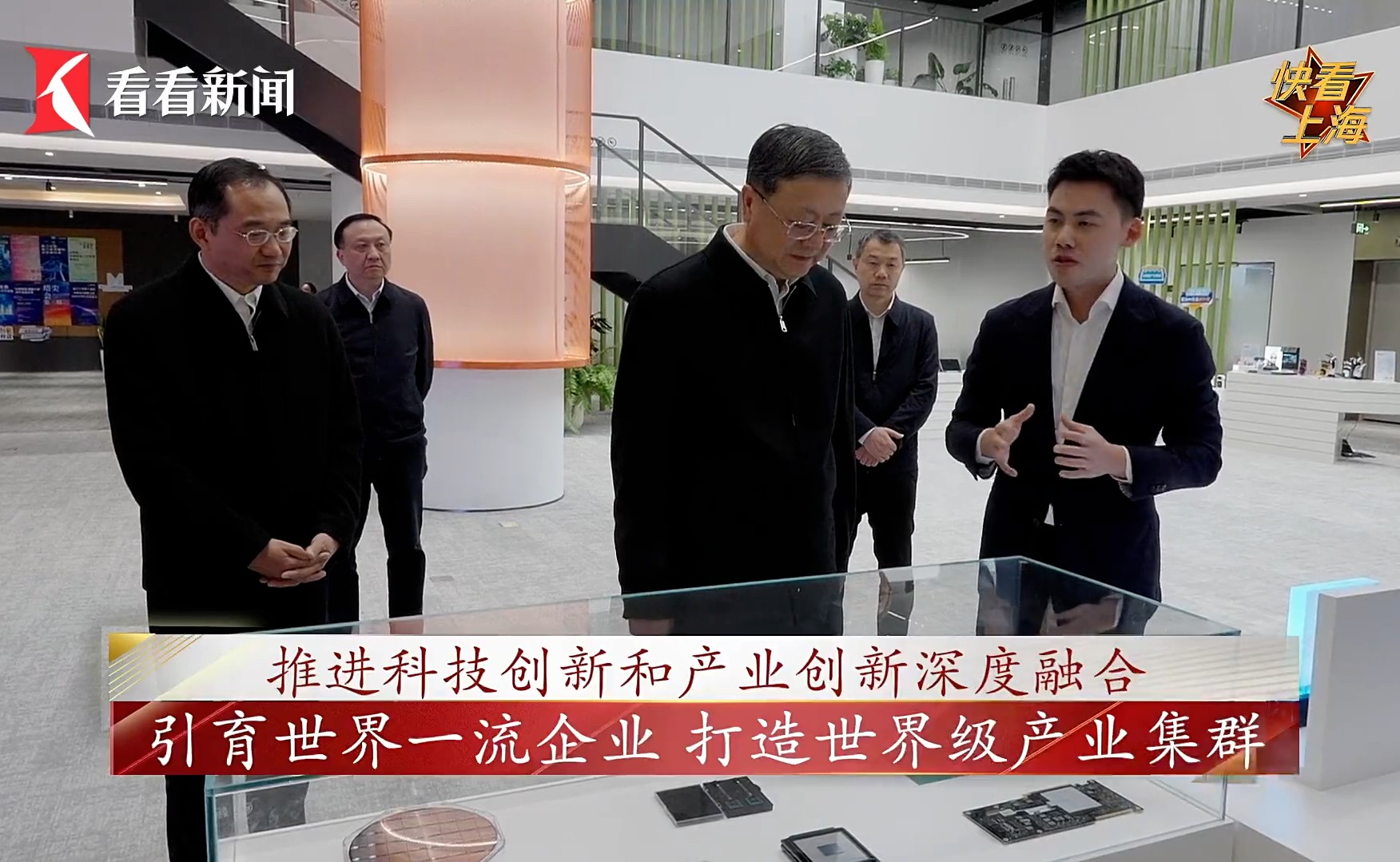
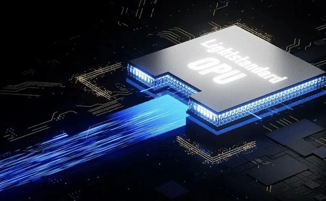
Lightstandard's glass optical computing chips better represent the future of AI computing. On January 4th, Lightstandard announced that it is using glass instead of silicon as a substrate to develop glass optical computing chips. Co-founder Cheng Tangsheng stated that this move will allow AI computing to bypass the problems of computing power growth relying on advanced processes and high computing power inevitably accompanied by high energy consumption, and enter the era of " thousand POPS-level computing power and thousand TOPS/W energy efficiency ratio ". On the same day, Chen Jining, Secretary of the Shanghai Municipal Party Committee, inspected Lightstandard's latest products, including glass optical computing chips, during a special research on technological innovation and industrial development in Pudong.
At the Saudi Industrial Transformation Exhibition in December 2025, Saudi Minister of Industry Bandar Khulaf praised Lightstandard's glass optical computing chip as representing the future of AI computing and invited Xiong Yinjiang, another co-founder of Lightstandard, to a closed-door meeting to discuss future cooperation. More than 700 international media outlets, including Egypt's Al-Masri, the Associated Press, NBC, Yahoo Finance, Morningstar, and British AI and Technology magazines, covered the meeting.
Lightstandard's optical computing products are primarily used in AI inference scenarios. It is projected that by 2030, inference will account for 75% of total AI computing, reaching a market size of $255 billion. While other startups are still struggling to raise funds, Lightstandard has completed five rounds of financing in just three years, attracting investment from three types of capital: leading VCs, domestic internet giants, and state-owned funds from Shanghai and Suzhou.
Beyond glass-based optical computing chips, Lightstandard has also proposed building a next-generation all-optical computing system based on glass-based optical computing. This system would complete all AI computing tasks through optical computing, simultaneously breaking through the ceilings of computing power, energy efficiency, and computational efficiency. Coincidentally, Shanghai Jiao Tong University has also recently achieved a breakthrough in the field of all-optical computing chips. This resonance between industry and academia clearly points to one question: Does this mean that AI computing is accelerating towards the "all-optical era," and a technological and industrial revolution, akin to "new energy vehicles," that could potentially disrupt the global AI computing competition landscape is officially underway?

▲ Xiong Yinjiang (left), another co-founder of Lightstandard, and Bandar Khuleif, Saudi Minister of Industry (right).
1400 times the computing power, 200 times the energy efficiency, and 650 million computing units of storage.
Prior to this, major optical computing companies worldwide, including Lightstandard, chose to manufacture optical computing chips using silicon as a substrate. This is because silicon photonics platforms are almost seamlessly compatible with existing CMOS processes. However, pure silicon modulation has many limitations. Therefore, it took three years for the matrix size to expand from 64×64 to 128×128. Lightstandard, which integrates phase change materials and silicon photonics heterogeneously for optical computing chips, broke through this bottleneck.
Cheng Tangsheng pursued his PhD in Materials Science and Engineering at Oxford University, where he led a team to develop novel phase change materials and achieve large-scale integration of phase change material optical chips. Why did Lightstandard choose to replace silicon with glass to once again ignite a technological revolution? In Cheng Tangsheng's view, this is to enable optical computing products to far surpass the performance of mainstream electrical computing products currently used for AI inference scenarios worldwide. Only in this way can AI computing usher in the "era of light."
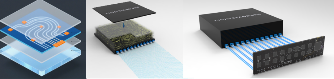
Glass possesses advantages such as flatness, thermal stability, broad-spectrum transparency, and compatibility with optical waveguide processes, making it considered the best material to replace silicon interposers and organic substrates in the development of semiconductor technology. International tech giants like Nvidia, Intel, Samsung, and AMD are all using glass to improve product performance. However, limited by the maximum mask size of lithography machines, the largest optical computing chip that can be designed using current silicon photonics platforms is 32mm × 25mm. Further increasing the area will lead to a continuous increase in design and manufacturing complexity with each subsequent iteration.
Using glass as the substrate for optical computing chips, the nanoimprint process can break through the exposure size limitations of existing silicon photonics platforms while maintaining chip precision, thereby accommodating more computing units, improving the computing power of a single chip, and making it easier to solve problems such as material warpage and waveguide loss when manufacturing larger chips in the future, greatly reducing the design and process difficulty of product iteration.
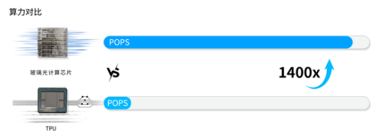
According to Cheng Tangsheng, a 200mm x 200mm glass optical computing chip can achieve a computing power of 2600 POPS, which is 1400 times that of Google's TPU and 1300 times that of NVIDIA's H200 (non-sparse) . Based on the demand in the AI inference market and the development trend of technology, the chip size is expected to increase several times over.
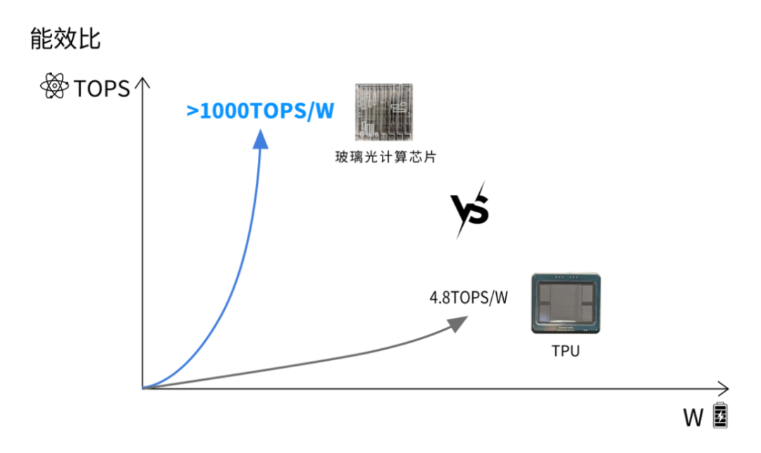
In terms of energy efficiency, Lightstandard utilizes the non-volatility of phase change materials to achieve zero static power consumption for its optical computing chip, requiring only one electrical drive to complete an AI computing task. Due to the extremely weak nonlinear optical effects of glass, the waveguide propagation loss of light is extremely low, allowing for the selection of low-power lasers in chip design. Furthermore, the advantages of glass in terms of dielectric loss, transmittance, flatness, and thermal stability can further reduce chip power consumption. Cheng Tangsheng predicts that the energy efficiency ratio of the 200mm x 200mm glass optical computing chip can exceed 1000 TPOS/W, equivalent to more than 200 times that of a TPU .
Glass-based optical computing chips can also solve the memory bottleneck faced by large AI models. Lightstandard utilizes the non-volatility of phase-change materials to achieve in-memory computing in optical chips. The chip's computing units are also storage units, capable of storing various parameters for AI calculations, breaking down the memory wall in the von Neumann architecture, where the amount of parameters stored depends on the size of the computing units. Glass-based optical computing chips can store even more AI calculation parameters; a 200mm×200mm glass-based optical computing chip can store 650 million computing units . Each token will complete calculations at the speed of light, eliminating the need for repeated readings of model parameters and achieving zero static power consumption.
Is glass-based optical computing a better path to achieving all-optical computing?
Cheng Tangsheng stated that Lightstandard has already verified the fabrication process of optical devices such as optical waveguides on glass. The waveguide loss has been optimized to a level lower than that of silicon photonics platforms. Simultaneously, they have conducted large-scale array sample fabrication and phase change material process optimization. Furthermore, they have integrated the upstream and downstream industry chains, collaborating with upstream manufacturers such as nanoimprint lithography to optimize processes, and establishing a two-way feedback mechanism for R&D and application with downstream large enterprises. The ultimate goal of Lightstandard in continuously seeking breakthroughs in materials and manufacturing is to directly package glass optical computing chips into ultra-high-performance all-optical computing systems, thereby gaining the right to define the next generation of AI computing technology standards.
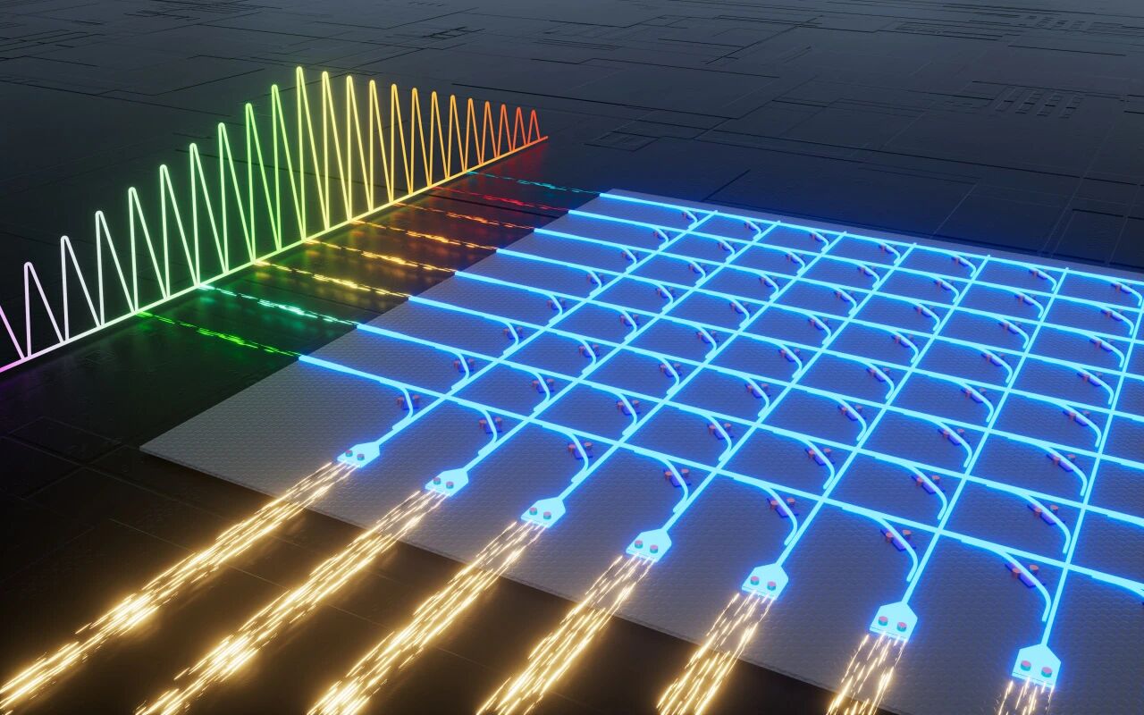
What is an all-optical computing system? It enables repeated computation and dynamic storage of optical signals within the optical domain, changing the current situation where optical computing can only serve as a "single computing core," and allowing glass optical computing chips to become AI computing platforms that directly run complete models.
Developing all-optical computing has become a global consensus in academia and industry. Its core significance is to overcome the energy consumption and heat dissipation bottlenecks of electrical computing, enabling a balance between ultra-high computing power and ultra-low energy consumption.
Before glass-based optical computing, there were two main approaches to all-optical computing. One approach was to implement optical logic gates similar to the AND, OR, and NOT gates of transistors on light. This approach required a group III-V platform with direct bandgap characteristics. Due to the characteristics of optical devices, the transistor density was not advantageous compared to CMOS. The other approach utilized the interference, refraction, and diffraction properties of optics to achieve integrated sensing, storage, and computing. The light signals collected by the optical sensor were directly input into the computing unit for calculation and output. This approach could not control the parameters of each pixel in real time, making the application scenarios relatively fixed. In contrast, the parameters inside the computing core of a glass-based optical computing chip can be adjusted in real time according to different models and requirements, making the application scenarios more comprehensive and flexible. Furthermore, since all-optical computing also needs to perform different calculations such as nonlinear operations, and different calculations require different materials or solutions, using glass, which has characteristics such as a smooth surface, low coefficient of thermal expansion, and low warpage, as a substrate makes it easier to integrate chips from different platforms, thereby realizing all-optical computing.
Regarding the future of optical computing, Cheng Tangsheng believes that glass optical computing chips will change the current "electric-dominant, optical-assisted" architecture of optical computing products, forming a computing cluster architecture of "optoelectronic integration, with optical as the primary element" or even "all-optical." Lightstandard's "vast vision" is to provide full-stack optical computing solutions covering all scenarios for different types of users. This ranges from providing C-end users with a glass optical computing box with 50P+ computing power , equivalent to a small home data center capable of powering humanoid robots, to providing large model companies with a "optical computing + optical connectivity" solution with 500P+ computing power , and even building a large data center with 5000P+ computing power for governments or large enterprises through a "optical computing + optical connectivity + optical transmission" solution . At that time, Chinese companies, including Lightstandard, are expected to win this "new energy vehicle"-style technological and industrial revolution that will rewrite the global AI computing competition landscape.
Recommended News
Recommended News
Recommended News